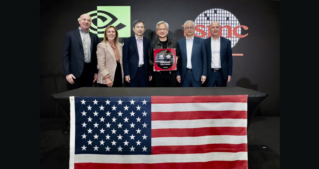
NVIDIA and Taiwan Semiconductor Manufacturing Co. (TSMC) produced the first NVIDIA Blackwell wafer on US soil, a milestone in onshoring high-end artificial intelligence chipmaking.
NVIDIA CEO and founder Jensen Huang was accompanied by the company’s executives to the TSMC new Phoenix facility to celebrate, signing the inaugural wafer alongside Y.L. Wang, TSMC’s vice president of operations, according to NVIDIA.
Huang called it “a historic moment,” saying that it was the first time in recent U.S. history where “the single most critical chip” is being produced in the United States. He defined the initiative as fitting into a larger vision of how to reindustrialize America and strengthen national supply chains.
Ray Chuang, CEO of TSMC Arizona, was amazed at how quickly the site had evolved, mentioning that three decades of collaboration have served as the foundation of the collaboration with NVIDIA. “To be able to come to Arizona and stand here today shipping the first U.S.-made NVIDIA Blackwell chip in a matter of a few years is the best of TSMC,” he stated in the blog.
The facility will produce future-generation semiconductors like two-, three-, and four-nanometer chips, and A16 designs used in AI, telcos, and high-performance computing.
The Blackwell wafer is the substrate that carries NVIDIA’s existing generation of GPUs, which are famous for their performance and power efficiency in AI workloads. NVIDIA said it will also infuse AI, robotics, and digital-twin technology into its upcoming U.S. factory lines.
Company leaders called the Phoenix milestone an important milestone towards building America’s AI infrastructure and ensuring long-term leadership in semiconductor innovation.
A global media for the latest news, entertainment, music fashion, and more.


